Shenzhenshi Shuangfengtai Technology Co.Ltd Welcome your visit....... Chinese   ENGLISH
Your location: Technology and services → Process Capability 
Maximum process capability
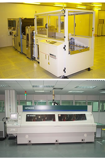
﹡Circuit board layers: 1-20 layers
﹡Minimum line width / space: 3mil/3mil
﹡Min drilling range: 0.15mm,laser 0.1mm
﹡Finished plate thickness: 0.20-7.0mm
﹡Impedance control range: + - 10%
﹡Surface treatment method: Hot air leveling, chemical immersion gold, silver, gold finger, full plate gold plating, lead-free tin spray、OSP
﹡Aperture ratio: 1:12
Long-term, on-time, and fast delivery capabilities Fast delivery templates can support your R & D process for a long time
1、2-6 floors (1-5 days)
2、8-10 floors (5-7 days)
3、12-20 floors (7-10 days)
 FriendLink:Baidu PCB Alliance Network PCB Forum Network PCB Technology Network PCB Information Network PCB Talent Network Communication PCB Huawei 
About Us Products Factory Tour Technology News Feedback Contact Us
WeChat Consulting
TEL:0755-29906588 FAX:0755-29906228
E-mail:md@latfpc.com Add:Bld 9, Wanan Road, Shayi Town, Shajing Town, Baoan District, Shenzhen
Copyright©2003-2024 SHEN ZHEN LAT PCB CO.,LTD. Design:Huawei  
PCB | PCB | PCB board | Communication PCB | PCB proofing | Automotive PCB | Security PCB | PCBA | PCB proofing | PCB circuit board
online service
Business:
Business:
Schedule: